Plasma box
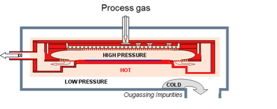
Choose Plasmabox for pinhole free, high purity films and simple reactor maintenance

Test Modal

Ullenda voluptaspe natem. Ceped quam rem. Nemped que porehen ihilitatis quas endest etur alis as id quatium expelic imoluptatur repe dendere ribus, sam nonserferum nessit que vel maxim re porro od quam dolo dusaectore aperuptae qui volore, comnisquo tem incto blacepu digniet pra dit labo. Tis aspid et everfer ovidestis derro tem sedis eicabo. Optaspe rferia volesenes erro quam, sitatus solut quiatum res same atem hitiam vento is videbit velit deror autatem.
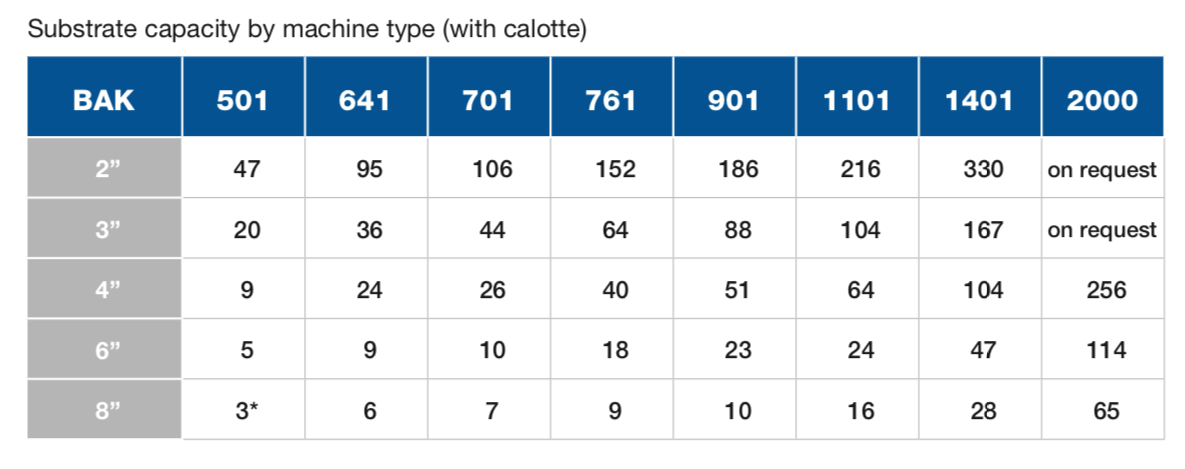
From the smallest to the biggest- get an idea how many substrates our systems can hold in a single batch


ETCH TECHNOLOGIES
Technologies for applications at wafer or panel level
Stand-alone etch processes at high and uniform rates pose one set of challenges, whilst improving the properties of excellent coatings even further by an additional plasma etch treatment set different ones. Within the broad field of etching metals or dielectrics, film densification, native oxygen removal, post-oxidization, ashing and sputtering, Evatec delivers custom source designs paired with dedicated process experience. Our production solutions all comes with one common goal of maximizing throughput and minimizing cost of ownership.
Dielectrics Etch
Film adhesion plays a critical role at the beginning of any surface processing. In particular, when depositing functional coatings such as optical filters on polymers, surface activation and native oxygen removal on CLUSTERLINE® 200 equipped with Evatec's batch process module technology and MSP pave the way for optimum results. Then, the best results of metal oxide coatings are achieved using our auxiliary plasma etch approach during the actual deposition process. Generating a plasma beam in our CCP sources and applying this beam with a controlled amount of ion energy to the growing film results in superior density, conformality/gap filling, and surface roughness – no other technology can reach the same levels of quality and quantity. This is the basis for the optimum solution for high volume manufacturing of the multilayer stacks used for optical bandpass filters, temperature-compensated surface acoustic wave (SAW) filters, and many other applications.
Metals Etch
Ion beam etching is the method of choice for evaporation applications on the BAK Platform.
Advanced Packaging
Dedicated ICP Arctic Etch technology available on CLUSTERLINE® 300 and HEXAGON platforms use ICP for high ion fluxes combined with RF substrate bias for adjustable ion energy. In combination with degas and sputter technologies the hybrid reactor enables stable contact resistance (Rc) values on highly outgassing organic substrates in typical applications like FOWLP. Where even larger surfaces need to be etched too, the Dual-Frequency CCP utilized in Evatec's CLUSTERLINE® 600. Platform drives any physical and chemical etching process turning Fanout and IC Substrate manufacturing on panel level scale into reality.
To learn more about our know-how and platforms click on the individual tabs or click here to contact us.
Inductively Coupled Plasma Technology
Choose Evatec ICP technology to benefit from the following features
- Optimized reactor design and driving frequency for purely inductive coupling of the plasma means that the process is operated at very high plasma densities and in a very reproducible way
- RF substrate bias for tuning the impact energy of the high ion current enables very high rates for any physical and chemical etching process
- Physical ion etching can be mixed with chemical etching with adjustable spatial distribution for selective etching through masks, from wafer center up to the edge
- Carefully developed wafer environment for clean process leads to cutting-edge particle performance
Capacitatively Coupled Plasma Technology
Choose Evatec CCP technology to benefit from the following feature
- Capacitively coupled plasma sources are a well-established type of thin film etcher technology providing reliable etching solutions based on extensive experience
- Our modern models are equipped with specifically chosen single- or dual-frequency RF supply systems, operated in continuous or pulsed mode providing optimum performance of etching processes for even the most ambitious applications
- Hardware designed for wide control range of ion energy and ion flux means you can be ready for the future by tuning the etching step to follow any changes in requirements
- Both etch rate and uniformity levels are kept in the percentage range at the same time by built-in options of magnetic or geometric “plasma shaping” acting as a robust solution with high yield and long uptime for favorable cost efficiency
- Surface treatment by quasi-neutral plasma beam with high energy at low voltage leads to minimum charge-up of sensitive layers or devices on wafer
Etch Platforms
Each of our platforms is equipped with a specific reactor design, tailored to the needs of the Advanced Packaging, Semiconductor, Optoelectronics and Photonics markets. Complementing our solutions for thin film deposition with plasma etching capabilities makes each a powerful tool with a complete set of thin film processing solutions.
Our experts are on hand to help you find the right platforms according. Alternatively, click on the photo links to read more about each platform.
BAK FAMILY
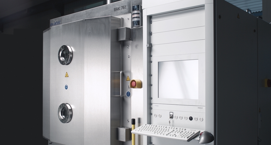
Flexible box coater range from 0.5 to 2.0 metres with manual or autoload offering a range of ion beam sources for energy impact and physical etching before, during, and after evaporation.
CLUSTERLINE® 200
Single Process Modules enabling ICP with RF bias for selective, damage-free etching of dielectrics and metals. Batch Process Module enabling CCP for stand alone etching or film treatment during growth.
CLUSTERLINE® 300
300mm cluster platform equipped with Single Process Modules enabling ICP etch with RF bias for selective high uniformity damage-free etching of dielectrics, TCOs and metals at high rates.
CLUSTERLINE® 600
Tool for FOPLP and next generation IC substrate processing of panel sizes up to 650x650mm. Integrates dual-frequency CCP source for fast and uniform etch prior to sputter deposition processes.
HEXAGON
Dedicated platform for advanced packaging applications like FOWLP offering ICP arctic etch with RF bias for preparation of highly outgassing organic substrates prior to sputter deposition.
LLS EVO II
Vertical batch sputter platform for semiconductor applications with manual or robot load integrating CCP technology for simultaneous etch of large batches of substrates.
SOLARIS® FAMILY
Family of high speed inline sputter solutions for ultra high volume production equipped with ICP etch for native oxide removal and surface cleaning prior to deposition.
Stand-alone etch processes at high and uniform rates pose one set of challenges, whilst improving the properties of excellent coatings even further by an additional plasma etch treatment set different ones. Within the broad field of etching metals or dielectrics, film densification, native oxygen removal, post-oxidization, ashing and sputtering, Evatec delivers custom source designs paired with dedicated process experience. Our production solutions all comes with one common goal of maximizing throughput and minimizing cost of ownership.
Dielectrics Etch
Film adhesion plays a critical role at the beginning of any surface processing. In particular, when depositing functional coatings such as optical filters on polymers, surface activation and native oxygen removal on CLUSTERLINE® 200 equipped with Evatec's batch process module technology and MSP pave the way for optimum results. Then, the best results of metal oxide coatings are achieved using our auxiliary plasma etch approach during the actual deposition process. Generating a plasma beam in our CCP sources and applying this beam with a controlled amount of ion energy to the growing film results in superior density, conformality/gap filling, and surface roughness – no other technology can reach the same levels of quality and quantity. This is the basis for the optimum solution for high volume manufacturing of the multilayer stacks used for optical bandpass filters, temperature-compensated surface acoustic wave (SAW) filters, and many other applications.
Metals Etch
Ion beam etching is the method of choice for evaporation applications on the BAK Platform.
Advanced Packaging
Dedicated ICP Arctic Etch technology available on CLUSTERLINE® 300 and HEXAGON platforms use ICP for high ion fluxes combined with RF substrate bias for adjustable ion energy. In combination with degas and sputter technologies the hybrid reactor enables stable contact resistance (Rc) values on highly outgassing organic substrates in typical applications like FOWLP. Where even larger surfaces need to be etched too, the Dual-Frequency CCP utilized in Evatec's CLUSTERLINE® 600. Platform drives any physical and chemical etching process turning Fanout and IC Substrate manufacturing on panel level scale into reality.
To learn more about our know-how and platforms click on the individual tabs or click here to contact us.
Inductively Coupled Plasma Technology
Choose Evatec ICP technology to benefit from the following features
- Optimized reactor design and driving frequency for purely inductive coupling of the plasma means that the process is operated at very high plasma densities and in a very reproducible way
- RF substrate bias for tuning the impact energy of the high ion current enables very high rates for any physical and chemical etching process
- Physical ion etching can be mixed with chemical etching with adjustable spatial distribution for selective etching through masks, from wafer center up to the edge
- Carefully developed wafer environment for clean process leads to cutting-edge particle performance
Capacitatively Coupled Plasma Technology
Choose Evatec CCP technology to benefit from the following feature
- Capacitively coupled plasma sources are a well-established type of thin film etcher technology providing reliable etching solutions based on extensive experience
- Our modern models are equipped with specifically chosen single- or dual-frequency RF supply systems, operated in continuous or pulsed mode providing optimum performance of etching processes for even the most ambitious applications
- Hardware designed for wide control range of ion energy and ion flux means you can be ready for the future by tuning the etching step to follow any changes in requirements
- Both etch rate and uniformity levels are kept in the percentage range at the same time by built-in options of magnetic or geometric “plasma shaping” acting as a robust solution with high yield and long uptime for favorable cost efficiency
- Surface treatment by quasi-neutral plasma beam with high energy at low voltage leads to minimum charge-up of sensitive layers or devices on wafer
Etch Platforms
Each of our platforms is equipped with a specific reactor design, tailored to the needs of the Advanced Packaging, Semiconductor, Optoelectronics and Photonics markets. Complementing our solutions for thin film deposition with plasma etching capabilities makes each a powerful tool with a complete set of thin film processing solutions.
Our experts are on hand to help you find the right platforms according. Alternatively, click on the photo links to read more about each platform.