
SOLARIS® S380
Inline architecture for 15inch diagonal
SOLARIS® S380
The "inline" SOLARIS® S380 offers easy tool configuration and scope for future expansion for multiple processes and substrate sizes. It handles carriers up to 15 inch diagonal. Proven manufacturing performance combined with easy size conversion provides excellent utilization and CoO.
Choose SOLARIS® S380 for selected high volume processes like chip scale EMI shielding or touch panel.
S380 – a quick guide
Click on the individual sections in the circle form a quick guide to major components and capabilities or read more details below
Vacuum
- Turbo molecular pumps combined with dry rotary pumps
- Ultimate pressure in the low E‑7 mbar range
- Each process chamber equipped with an individual pump
- Complete vacuum separation during processing
- Minimal cross-over during substrate transfer between chambers
Single PVD Source
- DC, DC reactive, or 13.56 MHz RF sputter sources available
- Large area single-target sources for high uniformity deposition on substrates top to 380mm diagonal
- Individual chamber venting for target exchange
PVD 3D Source
- Designed for three-dimensional coating applications
- Supports DC and DC reactive deposition processes
- Suitable for substrates up to 95 × 190mm (rectangular)
Etch Source
- Hard etching of metals and/or oxides
- Optional glow discharge cleaning station
- Removes organic residues from substrate surfaces
- Improves adhesion through surface activation
Cooling Source
- Rapid cooldown of heated substrates
- Performed in an individual dedicated chamber
- Prevents substrates from exceeding defined temperature limits
RTP Source
- Rapid substrate heating in an individual chamber
- Heating capability up to 400 °C
- Prepares substrates prior to coating processes
Process chambers
Equip the system with up to 5 process chambers configured for:
- Continuous substrate rotation during processing to ensures excellent angular uniformity across the substrate
- Individual chamber venting for fast target exchange
Substrate management
- Dedicated substrate carriers for specific substrate geometries
- Supports substrates of any shape
- Maximum substrate thickness up to 4mm
PVD Multisource
- Enables material engineering via simultaneous sputtering of different materials
- DC, DC reactive, or 13.56 MHz RF sputter sources available
- Any combination of up to four individual sources per chamber
System Concept and Architecture
The SOLARIS® S380 is optimized for high-volume production of larger substrates up to 15 inches.
It provides high throughput and excellent uniformity, making it ideal for EMI shielding, display applications and large-area conductive coatings.
- Inline substrate transport with synchronized carrier indexer
- Up to five process stations and a total of six chamber modules (incl. load/unload)
- Independent process modules for PVD, Etch or RTP
- Integrated carrier loading and unloading within the tool design
- Quick size conversion for flexible substrate formats via carrier exchange
Process and Coating Technologies
Each module operates independently, ensuring repeatable results in 24/7 production.
- PVD: DC, DC reactive or RF sputtering with chamber & shield cooling
- Etch / Activation: pre-clean or plasma surface treatment
- RTP: inline annealing up to 400 °C
- Multisource sputtering: up to 4 cathodes per chamber
- Substrate rotation for < ± 2..3 % uniformity (depending on material/process)
- Typical materials: SiN, SiO₂, Al₂O₃, ITO, TiO₂, Al, NiV, Ag, AuGe, Zn:AlO and alloys via MSQ multisource
- Penta Plus cathode technology for excellent step coverage and reduced target change time in EMI shielding applications
Modularity and Upgradeability
- Add or exchange process modules for PVD, Etch or RTP
- Handle substrates or carriers up to 380 mm diagonal
- Target and shield change ≤ 60 min
- Independent chamber operation for multilayer flexibility
Typical Applications
- EMI Shielding – wafer- and panel-level coatings using Evatec’s Penta Plus cathode technology for superior step coverage and film uniformity
- Touch Panels & Displays – large-area transparent conductive films (TCO / ITO)
- Photovoltaics – transparent and metal coatings for high-efficiency cells
- Optoelectronics – multilayer dielectric coatings
- Power Devices – thick metal deposition and contact formation
Read more about the SOLARIS® S380 in our LAYERS magazine
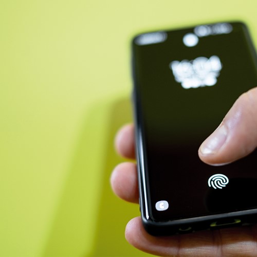
How does my Smartphone recognize me?
Biometrics is the science of measuring and analyzing biological characteristics and biometric methods are in common use today to authenticate our identity. In particular, fingerprint or face recognition are chracteristics that are used to secure access to personal devices like our mobile phones and Evatec’s production tools are already in use for exactly this type of application around the world today.